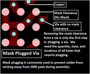
With a mask plugged via, (Mask Filled or Non-Conductive Filled via), specific measures are take n to ensure the via is plugged and sealed with mask and the annular ring is covered. A common application for this is on a BGA design where vias are commonly found in very close proximity to the BGA’s SMD pads. The concern is during assembly, solder will wick away from the intended pad and flow down the via creating poor or non-existent solder joints.
Plugged Via (Via Plugging)
Type A: sealing with a non-conductive material on one side, which partially enters the via.
Type B: sealing with a non-conductive material on both sides, which partially enters the via
Plugged & Covered Via
Type A: sealing with a non-conductive material on one side, which partially enters the via and additional covered up with solder mask
Type B: sealing with a non-conductive material on both sides, which partially enters the via and additional covered up
with solder mask
TIP: If you require mask plugged vias, this must be specified in your fab print or readme.txt file. We will need to know the quantity, sizes and locations of the vias to be plugged so we can be sure all the required holes are plugged.


